SPIE Advanced Lithography + Patterning 2026
LAB14 will be exhibiting at SPIE Advanced Lithography + Patterning 2026, one of the leading events for advanced manufacturing technologies.
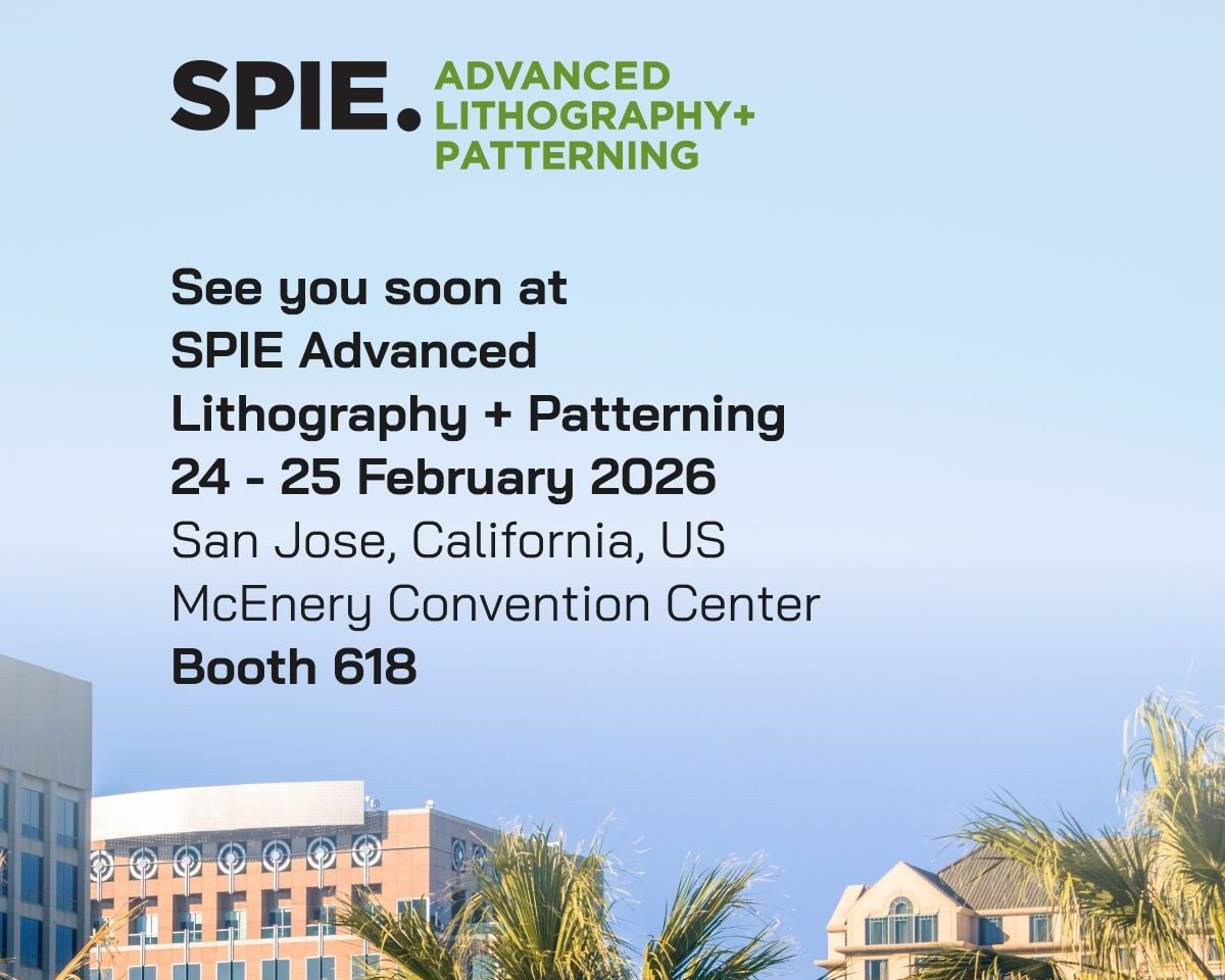
The conference and exhibition will take place on February 24–25, 2026, in San Jose, California, and brings together the global lithography and patterning community from research and industry. At Booth 618, LAB14 will present its expertise alongside with its subsidiaries Nanoscribe, GenISys, Notion Systems, and Nanosurf. In addition, Heidelberg Instruments will be exhibiting nearby at Booth 622, enabling visitors to explore complementary solutions within the SPIE Advanced Lithography + Patterning 2026 exhibition area.
Technology Exchange at SPIE Advanced Lithography + Patterning 2026
The conference serves as a key platform for discussing current developments in lithography, patterning, metrology, and process integration. The event facilitates in-depth technical exchange between researchers, system providers, and semiconductor manufacturers.
For the group of LAB14, participation s an opportunity to engage with existing partners, initiate new collaborations, and discuss application-driven system solutions in micro- and nanofabrication.
Meet LAB14 in San Jose
Visitors are invited to meet the LAB14 team at SPIE Advanced Lithography + Patterning 2026 to discuss current challenges and future directions in semiconductor process technology. Further information on exhibited topics and on-site activities will be published ahead of the event.